Gaptronics: Mechanical modulation
Active width control of nanogap lines will expand functionalities of the nanogap technology because the optical and electrical features of a nanogap are highly dependent on the gap width. We are innovating the active control method and named it ‘gap-tronics’. What is different from the existing breakjunction-based technologies is that we control lines of nanogap rather than a single contact point ensuring substantial light-nanogap interaction in a scalable manner up to wafer-scale devices.
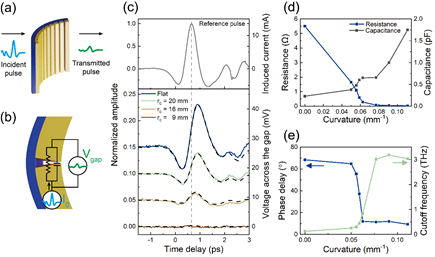
Mechanical deformation, the most intuitive way of gap width control, can be achieved by taking advantage of an elastic or flexible substrate. We fabricated nanogap slits on a PET substrate and demonstrated repetitive opening and closing, and consequent light modulation by bending the substrate.
Now we are developing an optomechanical/electromechanical width control method with various nanogap structures and substrates.
Wafer-scale active gap width control
Adv. Opt. Mater., 2002164 (2021)
Modulation of optical and electrical features
Nano Lett. 21, 4202-4208 (2021)