OVERVIEW
Research subject
We aim to extend the device footprint of nano/zerogap from the tip-based 1 nm^2 to the wafer-scale of 1 cm by 1 nm, to provide a viable platform for the real-world application of nanotechnologies.
We want to calibrate nano-scale gap change with millimeter-scale control movement, to directly connect the atomic scale world to the macroscopic world. Using a flexible substrate, we are varying nanogap width through mechanical modulation. Colossal light-matter interaction modification occurs when we change the gap width in real-time on the nanometer scale. By changing the microscopically small gap structure by the optimized mechanical control, we ultimately aim to realize an active device using the flexible nanogap, such as a molecular sensor, light shielding, and modulation device.
The studies about the flexible nano/zerogap are expected to provide a viable platform for the commercial application of nanotechnology. The flexible nano/zerogap active device will be directly applied to the industrial fields as well as fundamental studies such as low-dimensional materials, biomolecules, next-generation transistors, hydrogen energies, secondary batteries, 6G communications, etc. Additionally, the flexible nanogap active device can be manufactured in the industry by using an improved fabrication from the atomic layer lithography, the basic method of nanogap fabrication, which is expected to lead to its commercialization beyond the academic realm.
Group leader (Dai-Sik Kim)
- Distinguished Professor, UNIST, 2019~
- h-index: 62, Total citations: about 13,000
- Alumni: 34 of Ph. D., 19 of M.S, out of whom 18 became professors.
- Google Scholar: https://scholar.google.com/citations?user=bQxexEAAAAAJ&hl=en
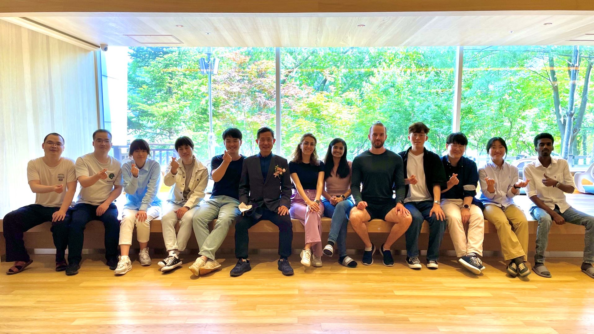
Who we are
- 15 Researchers with 2 Staffs
- Full support for equipment/research finance/administrative works so that researchers can focus only on ‘research’
- Diverse cultural/regional/academic backgrounds and Respect each individual's lifestyles